What is NVLINK?
The NVIDIA® NVLink™ is a high-speed GPU-to-GPU interconnect, that allows the GPUs to communicate directly with each other without relying on the slower PCI Express bus. This wire-based communication protocol was first introduced by NVIDIA in March 2014 and uses a proprietary high-speed signalling interconnect (NVHS). At a basic level, NVIDIA’s NVLink allows for the pooling of resources from multiple GPUs in such a way that allows one to access the memory and CUDA cores as though they were a single card which is great. For example AI, for scientific and rendering applications can benefit from this increased address space.
A bit of history…
The NVLink is an evolution of NVIDIA’s SLI (Scalable Link Interconnect) technology that was introduced back in 2004. SLI allowed for connecting two, three or four NVIDIA GeForce graphics cards to share the workload when rendering 3D computer graphics, typically in gaming. In order to configure the SLI, multiple graphics cards installed in a PC had to be linked together with a connector called SLI Bridge. Additionally, the motherboard inside the PC had to be certified by NVIDIA to ensure the things will work properly out of the box.
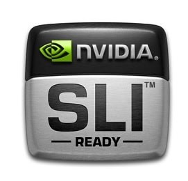
Pic1: NVIDIA SLI Ready logo that was present on motherboard boxes, supporting this technology.
In SLI, the graphics cards worked in master-slave configuration, all cards were given equal workload, however the final output of each card was sent to the master card which outputs to the monitor screen.
Two main modes of the SLI were Split Frame Rendering (SFR) and Alternate Frame Rendering (AFR). With SFR, the “master” card rendered only the top of the frame, the “slave” rendered the bottom part of the frame and, once finished, it was sent back to the “master” which combined both chunks of the frame before displaying it on the monitor.
With AFR, each graphic card worked on different frames, for example the first card rendered odd frames, the second card even frames which were then sent to and output by the “master” card. SLI offered up to 1.9x performance of single card in dual GPU configuration, however not all game titles were able to benefit from this technology, so the scaling performance would vary.
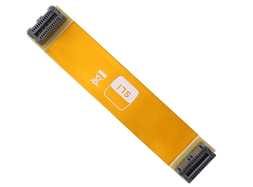
Pic2: SLI Bridge
As a result, the SLI technology was not perfect and the performance gain was often much lower than 1.9x, sometimes it caused visual artifacts on the screen. It required developers to put more time and effort into optimising the games for multi-GPU support, so they started moving away from it and optimised the games for a single GPU instead.
In September last year, along with the launch of the then new GeForce RTX™ 3000 series GPU’s, NVIDIA announced the end of SLI, so motherboard manufacturers and game developers might no longer support it.
NVLINK vs SLI – what is the difference?
The main differentiator is the speed – the SLI offered bandwidth of 1GB/s using the standard bridge and 2GB/s using a high bandwidth bridge. For comparison, the current 3rd generation of NVLink offers a total bandwidth of 600GB/s which is almost 10x greater that PCIe 4.0!
Unlike SLI, the NVLink bandwidth is bi-directional meaning that it does not use master-slave method, instead connecting the GPUs in a mesh network with multiple high performance links, allowing every GPU on that mesh to inter-communicate and pool resources.
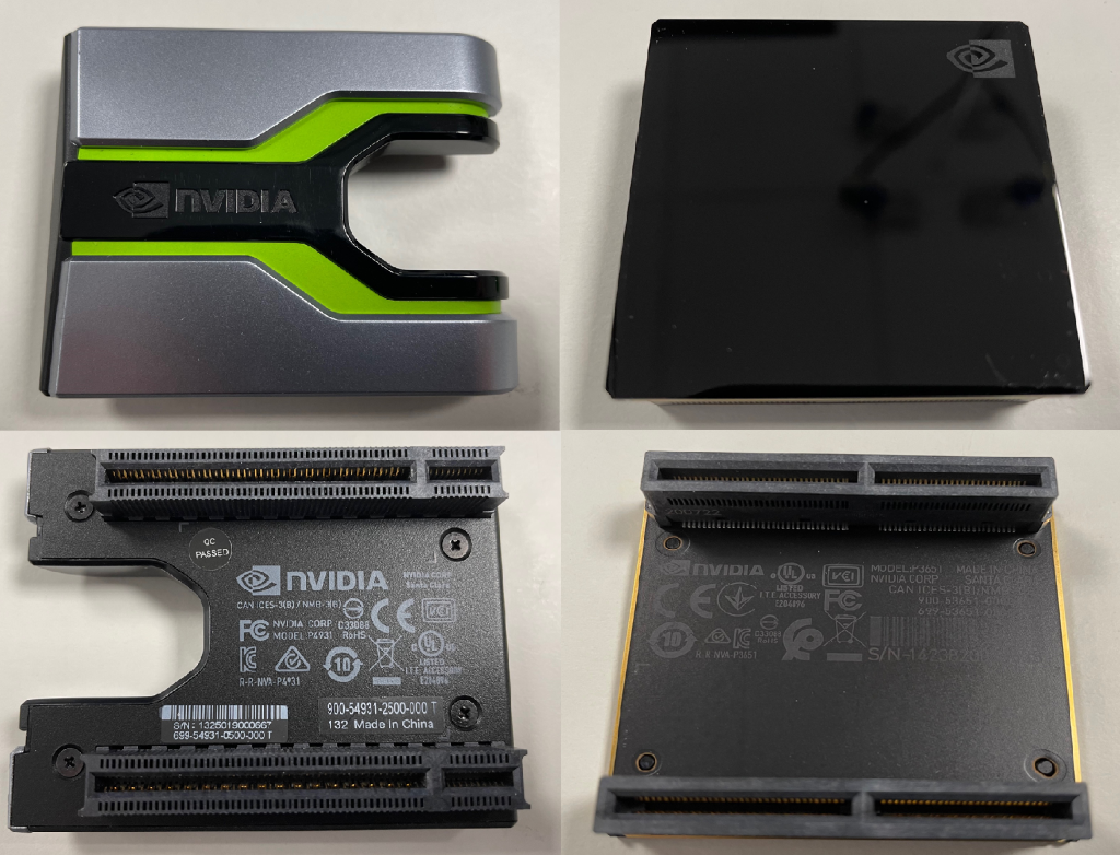
Pic3: 2nd generation (on the left) and 3rd generation (on the right) of NVLink bridge (source: Boston Labs)
Like SLI, NVLink uses physical interface bridges for GPUs that come in the standard PCIe FHFL card form factor and allows one to link two or three GPU’s together depending on the model. However, in some more dense server solutions that use the SXM4 form factor, NVLink is built-in to the multi-GPU board such as the NVIDIA HGX platform that powers their latest DGX A100 8-GPU supercomputer.
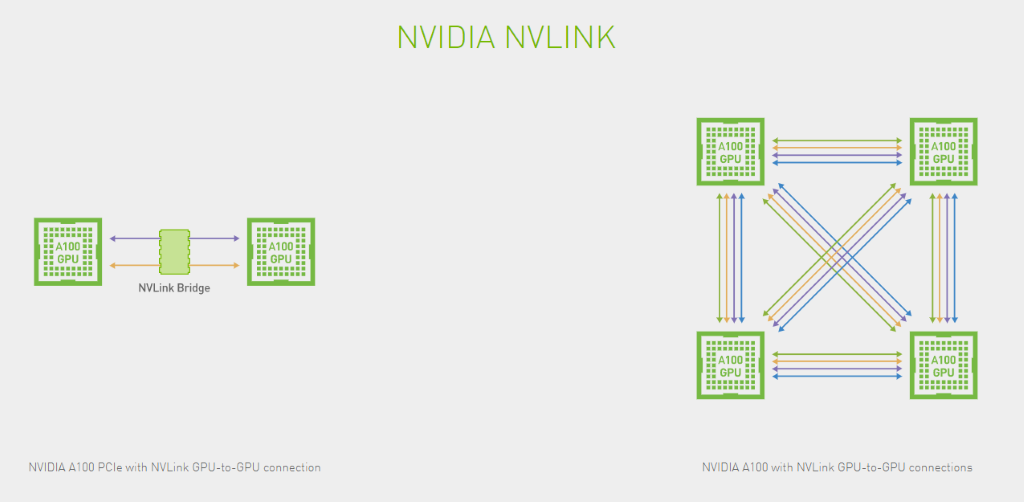
Pic4: NVLink for A100 PCIe (on the left) vs NVLink topology diagram for the A100 SXM4 GPU’s.
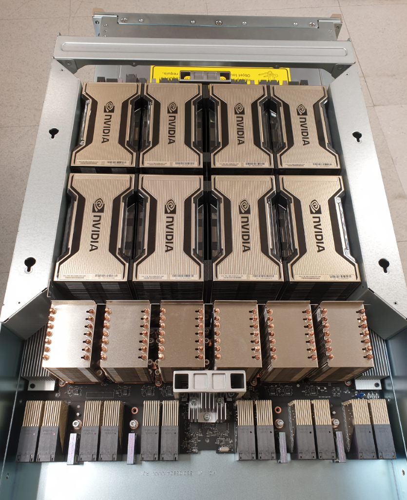
Pic5: NVIDIA HGX GPU board from DGX™ A100 populated with 8x A100 (source: Boston Labs)
3rd gen of NVLink for PCIe tested at Boston Labs!
The first generation of NVIDIA NVLink was introduced back in 2014 along with the Pascal architecture which then evolved into the second generation with the Volta architecture. Most recently, with the launch of the new Ampere architecture, NVIDIA have announced the 3rd generation of their GPU interconnect that is supported in their professional A-series GPUs such as the A100, RTX A6000 and A40 as well as the consumer grade GeForce RTX 3090.
Our engineers at Boston Labs took their time to test a pair of NVIDIA A100 PCIe 4.0 GPU’s that use 3 physical NVLink bridges (which are required for the best bridging performance and balanced bridge topology) and compare them with other Ampere GPU’s like RTX A6000 and GeForce RTX 3090 that support only 1 NVLink bridge.
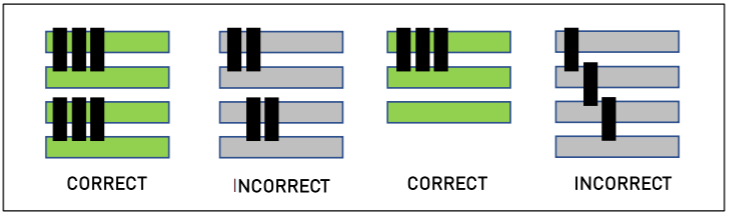
Pic6: A100 NVLink bridging topology (source)
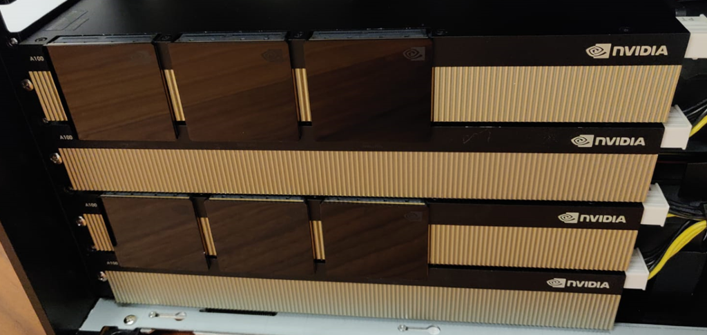
Pic7: 4x A100 PCIe GPU’s, connected with 3 NVLink bridges in pairs, installed in the workstation at Boston Labs (source: Boston Labs)
As a benchmark, we have used the Peer-To-Peer Bandwidth test from CUDA 11 toolkit.
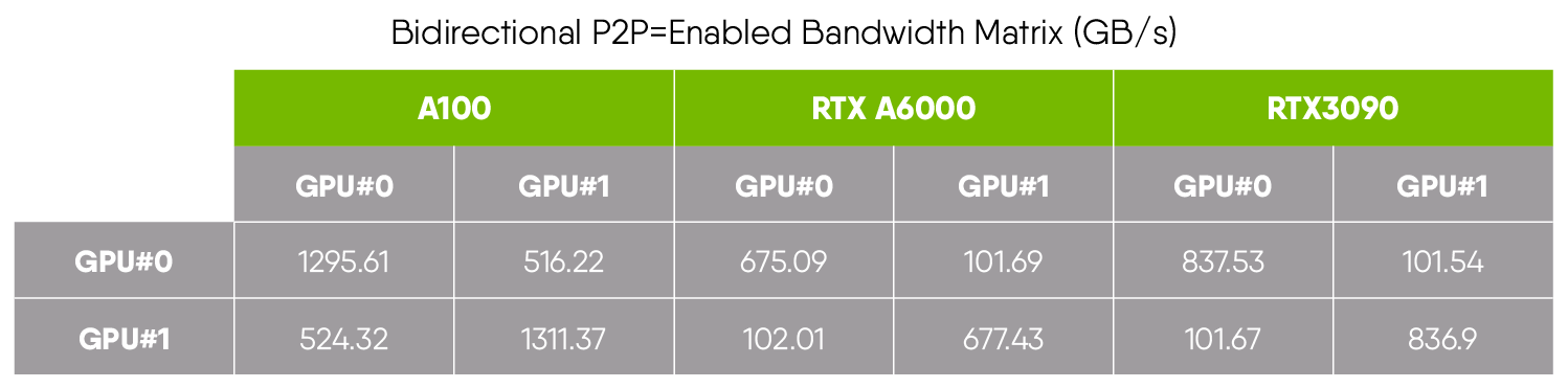
As expected, the A100 showed the best results thanks to 3 NVLink bridges and the fastest HBM2e memory, followed by the GeForce RTX 3090 that is using GDDR6X memory, then RTX A6000 with slightly slower GDDR6.
NVLink applications and conclusion
NVLink is a great technology, however, a popular Jensen Huang’s quote “It just works” does not fully apply here; software developers must implement the NVLink support into their application to take full advantage of it. Some of the renderers, scientific and AI applications are already supporting NVLINK, a few examples of these being:
- AutoDesk Arnold
- V-Ray
- AMBER
- Ansys Fluent
- Lattice QCD
There are many more and new ones being added all the time.
Boston Labs is our onsite R&D and test facility where we develop new products and evaluate the latest technology. New and improved technologies are emerging all the time, and this can be a daunting situation for customers planning their future projects. Making the right decision about new hardware is a difficult proposition, made even harder when clients are unable to test and understand the hardware first before making their purchase. Boston Labs enables our customers to test-drive the latest hardware on-premises or remotely. All the NVIDIA technology mentioned in this blog, such DGX A100, NVLINK, A100 PCIe, RTX A6000 is available for testing right now!
Boston Limited has been providing cutting edge technology since 1992. We offer many server and workstation solutions that support NVIDIA NVLink technology and can be tailored specially to your needs. If you would like to find out more, you can contact a member of our sales team.