
Contents:
- Boston finds AMD Rome having already visited Naples
- History where we have come from and where we are going to with AMD?
- Cheat sheet features list of Rome (Zen 2) per CPU
- Comparison between Naples and Rome
- Closer look at new CCX design designed for Zen2
- Memory/IO Die architecture diagram
- Summary of key CPU extensions with generation 1 and 2 of EPYC
- CPU Extensions enabled within Naples and now Rome
- CPU Extensions enabled within Rome
- Security features and vulnerabilities
- Upgrade path and considerations going from Naples to Rome with Supermicro
- Naming convention for CPU EPYC/EPYC SKUs
- AMD EPYC Gen 2 CPU SKU Range
- Boston AMD EPYC Gen 2 available at launch
History where we have come from and where we are going to with AMD?
AMD shook up the CPU industry when it released the first EPYC™ generation 7000 series (codename Naples) of processors and is looking to do the same with its second generation of EPYC 7002 series codenamed Rome.
Some people in the marketplace will look at the first generation and think we have been here before. To understand the potential userbase in trepidation we must look at the history of AMD and of their main competitor, Intel®. AMD brought out the Athlon 64 and Opteron 64bit (K8) processors in 2003 which changed the processor landscape at the time. Going from 32bit to 64bit and bringing dual core processors at a time when neither was available from Intel. Unfortunately for AMD this lead did not last, and Intel brought out the Intel Core microarchitecture. This started in late 2005/early 2006 with the Pentium M, Core Solo and Core Duo. Core 2 followed in late 2006/early 2007, introducing 64-bit extensions.
AMD's next generation to combat this known as Phenom arguably did not keep pace at this stage AMD stayed behind Intel until June 2017 when AMD EPYC 7000 (Naples) series launched. EPYC provided a lower price point and higher performance level than the Intel equivalent in some workloads.
AMD's EPYC 7002 Series to EPYC generation (Rome) builds upon the progress made by AMD in this market, and looks to blow away any reminders of the previous pattern seen. This is a big part of why Rome is so important since it proves that AMD can do multiple generations of performance and technology enhancements while showing a full roadmap for the future.
AMD EPYC 7000 generation we previously launched this series here and here.
Cheat sheet features list of Rome (Zen 2) per CPU
Here is an overall of what is possible
- Up to 64 cores
- Up to 128 Threads
- Up to 3.1GHz Base Frequency
- Up to 256MB of L3 Cache
- Up to 225W TDP
- 8 Channels of DDR4-3200
- Up to 4TB per socket of memory capacity using 256GB DIMMs
- No Chipset
- 128x PCIe 4.0
- 7nm lithography
- Infinity Fabric Gen 2
Comparison between Naples and Rome
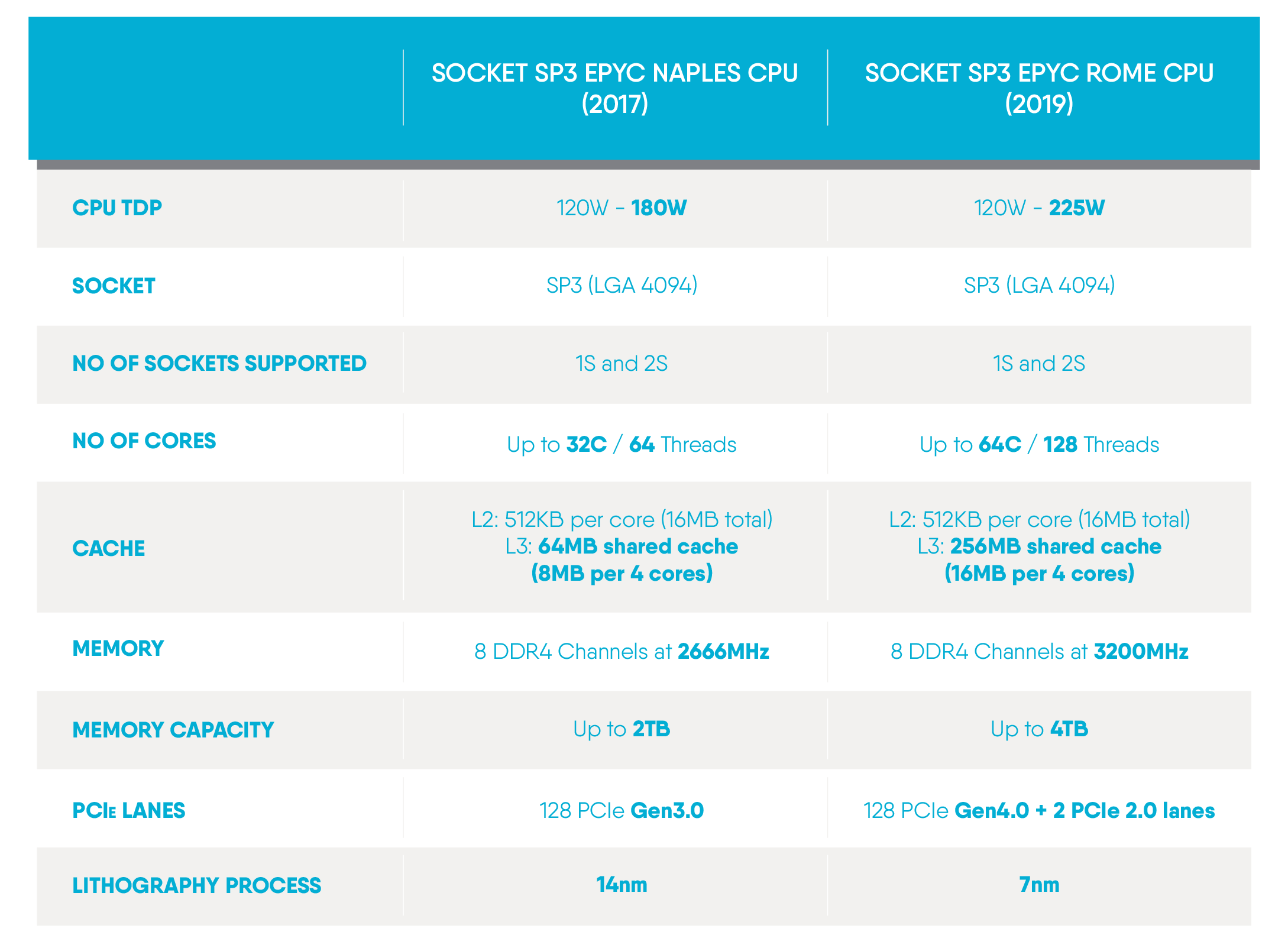
Here is a feature comparison between Naples on the left and Rome on the right. As you can see from the Die comparison pictures below there have been significant changes. This has come from the creation of the CPU complex architecture (CCX), Memory I/O die and a major change from the architecture of the first EPYC processor.
Closer look at the new CCX design designed for Zen2
At first glance you would assume that all the dies seen below are CPU cores with SOC as was the case with the 1st generation, however this would be incorrect as of the second generation. The CPU cores are now split.
1st generation of EPYC with the heat spreader removed:
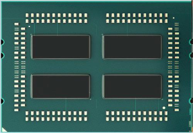
In the first-generation Naples utilised four System on chip (SoC) dies each with 8 cores and these are interconnected with AMD infinity fabric.
2nd generation of EPYC with the heat spreader removed:
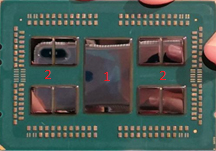
In the second-generation Rome, things have changed from the original EPYC design. While previously as above you had the SoC's, this has now been separated out for improved scale out architecture which AMD calls CCX and memory I/O die. The largest die shown is a memory/IO die (the red "1" in the picture) which provided all the functionality of the SoC apart from the CPU cores. These are the smaller CCX to the left and right of the big Memory/IO die in the middle (the red "2" in the picture denotes the CCX).
Memory/IO Die architecture diagram
Here is the CPU topology diagram for a 2 socket AMD 7002 series system and, as can be seen, there are many changes from the previous 7001 generation of EPYC.
Memory control is now centralised per socket since AMD have done away with the SoC design. EYPC 7001 had 4 NUMA nodes per socket for 8 in total with a dual processor system. NUMA topology can have a negative performance impact if the application is not NUMA aware. More importantly for AMD, Intel`s competing Xeon scalable products had two NUMA nodes per socket which is what most operating systems and applications will have been optimized for. AMD`s EYPC 7002 product now supports 2 NUMA nodes per socket which is a resulting benefit of the Memory / IO Die shown above.
The CPU cores themselves are separate and each CCX is 8 cores connected to 16MB of on-die Level 3 cache.
PCIe is now implemented with Up to 64 + 32 + 1 lanes per socket and Up to 16 PCIe lanes can be enumerated as SATA per socket.
Inter communication between CPU sockets is handled by Inter-chip Global Memory Interconnect 2 (XGMI-2) links. There are 4 XGMI-2 links shown in the diagram above: three of these are used by the CPU`s to “speak” to each other and the remaining 1 link per socket “feeds” 16 PCI-E lanes. Only one socket uses the 4th XGMI-2 link to break out into SATA.
Summary of key CPU extensions with generation 1 and 2 of EPYC
While each CPU generation is all about cores, threads and frequency, when you dig deeper there are further enhancements that come in the form of extensions. The purpose of an extension within the CPU architecture is to extend the functionality outside of the default instruction set and the functionality will be customised towards solving the targeted workload more efficiently than can be done otherwise.
Improving efficiently is not the only use case and in some scenarios will enable the CPU to process workloads that it could not otherwise do or to enable a feature that the CPU could not previously support.
AVX2 (Advanced Vector Extensions 2) is the second generation of AVX and both generations are supported on AMD EPYC. AVX additionally performs the instructions introduced with SSE extensions. SSE extensions were, in turn, an evolution of MMX, which could do two 32-bit floating point operations in one instruction. SSE doubles this to 4 and AVX offers up to 8 FP 32bit operations. AVX2 brought further improvements expanding the number of vector integer SSE and AVX instructions to 256 bits.
While all these mathematical operations may sound impressive: they may not mean much to the average user other than a box to tick. What does this really all mean to you?
In the CPU industry increasing Frequency, cores and threads can only get you so much performance as there are inherent issues in scaling these factors, frequency in particular. Adding these workload extensions allows for more operations per instruction. Each CPU core will have a certain level of IPC (instructions per cycle), sometimes known as Instructions per clock. This is what ultimately determines what is commonly known to most as single-threaded performance (and then scaled up with cores/threads to give multi-threaded performance).
However, it is not all down to having these supported in hardware since these instructions must be called or written into the software that you use to see any benefit. Not only must Operating Systems have support for the extension, applications will need this support too. Many well-known software packages already support AVX2 and, whilst this is not an exhaustive list, here are some examples of supported software platforms (the version listed or higher) that support AVX2 (as of the date of this article): Cinema 4D, Pixar’s Renderman 22.5 (onwards), Google’s Tensorflow, Ansys Fluent 18.1 and Gaussian 16. Previous software versions did not necessarily implement the AVX2 extension and this is partially why performance can change significantly between program versions.
CPU Extensions enabled within Naples and now Rome
- Simultaneous Multi-Threading
- AVX, BMI, F16C, FMA, SSE2/3/4
- AVX2, BMI2, MOVBE, RDRAND
- ADX, RDSEED
- Virtualisation Acceleration IOMMU
- Advanced Interrupt Virtualisation
- Nested Virtualisation
CPU Extensions enabled within Rome
- CLWB = Cache Line Write Back
- GMET = Guest Mode Execution Trap
- PQE/PQM Cache Allocation Technology and Platform QoS Monitoring
- VIOMMU = Virtualised IOMMU
- WBINVD = Cache Line Write Back and Invalidate
- WBOINVD = Cache Line Write Back without Invalidate
- X2APIC
Security features and vulnerabilities
AMD have several technologies and updates baked into EPYC generation 1 and 2: Secure Encrypted Virtualization (SEV), AMD Secure Memory Encryption (SME), AMD Secure Encrypted Virtualisation-Encrypted State (SEV-ES) and mitigation of side channel attacks. All with the express goal to improve overall system security whilst ensuring dependable system performance.
Further information on these topics can be found here.
Upgrade path and considerations going from Naples to Rome with Supermicro
Generally, between incremental generations of CPUs which are ‘Pin to Pin compatible’, a BIOS update to support the new CPU will be necessary. For the Rome upgrade from Naples there are several caveats that are covered in this section.
Naples to Rome is ‘pin to pin compatible’ meaning that you can install a EPYC Generation 2 CPU into a EPYC Generation 1 CPU era motherboard mechanically however due to the updated BIOS ROM size increasing between the two generations, memory speed increasing and with the arrival of PCI-E generation 4.0, various hardware changes are required.
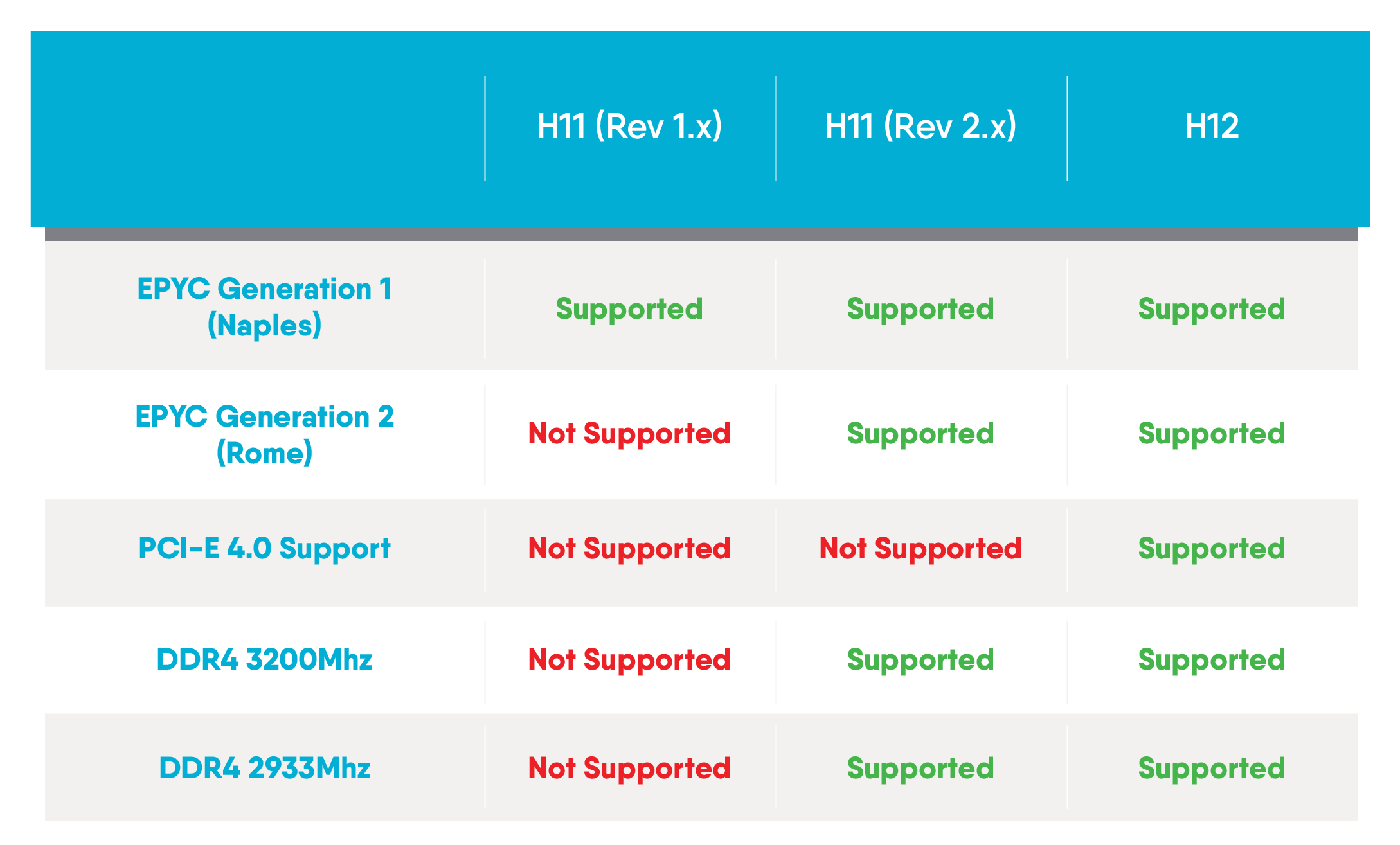
Here is the full guide of supported features for EPYC Gen 2 and the respective Supermicro motherboard generations:
If you have any concern or confusion about your upgrade path, system architecture, your required features or what revision of hardware you currently have, we are happy to help. When purchasing systems with us here at Boston, let us know your requirements and we can direct you towards the right system for your requirement.
Naming convention for CPU EPYC/EPYC SKUs
EPYC 7502P
- 7502P Processor Range: 7=EPYC/EPYC2 server processor
- 7502P Model Number: The higher the number generally indicates higher performance, no direct line to CPU specification
- 7502P Generation: 2=Rome (1=Naples)
- 7502P Feature: P=Single processor use only (cannot be used in a dual processor system)
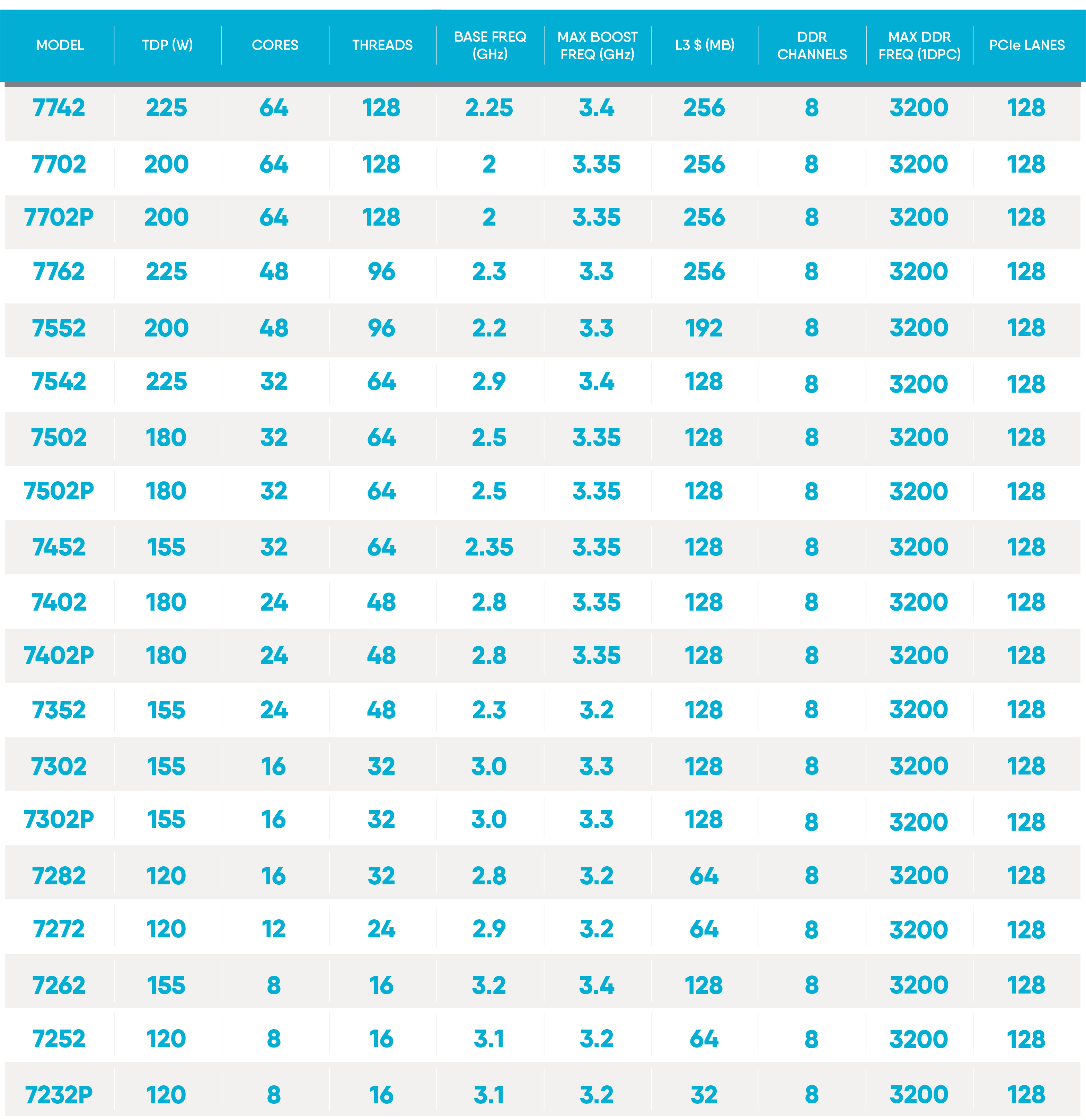
AMD EPYC Gen 2 CPU SKU Range
Boston AMD EPYC Gen 2 available at launch
You can view our Boston Quattro 12256-T02 which includes AMD EPYC™ Gen 2 here or download the datasheet here.
If you would like more information or design and architecture help around AMD's 2nd Generation of EPYC processors, then we'd be keen to hear from you. You can get in touch below:
Further information on AMD's 2nd Generation of EPYC and 1st Generation of EPYC can be found on our website here.